S100 Computers

Home S-100 Boards History New Boards Software Boards For Sale
Forum Other Web Sites News Index    
  
An S-100 68000 CPU Board.
   
  68K CPU Board V3
Introduction
A few of the later S-100 board manufactures had their own 68000 CPU card.  Amongst the best well known were the ones by CompuPro and  Dual Systems Peak Electronics had an 8 bit 68008 CPU board and Cromemco even went as far as a 68020 board.  I have little information on the latter two boards however.

The Motorola 68K represents the "other side" of the great software divide for desktop systems.   In the early 8 bit days there was a continuous tug of war between the Intel/Zilog camp and the Motorola camp.   This later evolved into the PC based 8086, 80286, 80386, 80486 and Pentium based systems. The Motorola camp, Apple/Sun based , evolved into 68000, 68020, 68040 based systems. See here for a brief historical summary.

I have to admit that up until now I have always found myself in the Intel camp, both in terms of hardware and software.   From a hardware perspective there are some very significant differences how Intel and Motorola CPU's talk to the world.  Somewhat oversimplifying, one could say that Intel CPUs assume that external devices are ready to talk to them immediately unless told otherwise (adding wait states).  While Motorola CPU's assume the opposite, they wait for a "I'm ready to talk" signal unless they are told otherwise -- so called synchronous communications.

When we look at the S-100 bus signals it is clear that it is setup for Intel style chips -- this really has to do with the bus's origin an 8080 CPU.  To insert a Motorola 68K CPU board therefore on the bus one has to take care shoehorning the CPU signals in carefully.

The Motorola 68K CPU turned out to be a very popular microprocessor. It was the basis of Apples Mackintoshes desktop line.   A number of people saw the need for an S-100 based 68K CPU board.  However these boards are very rare today.   There is a need for a new S-100 based 68K CPU board.   Furthermore it would really be nice if such a board could take advantage of the IEEE-696's bus standards to allow the board to co-exist with other CPU's on the bus.  One could for example switch from a Z80 (or 8086) to the 68K board and back again in software.  Unfortunately I know of no 68K board that had this capability. All the above 68K CPU boards ran a single "bus masters".  We will try and incorporate this master/slave capability in our new board (more on this later, see below).      
Wilcox Book  
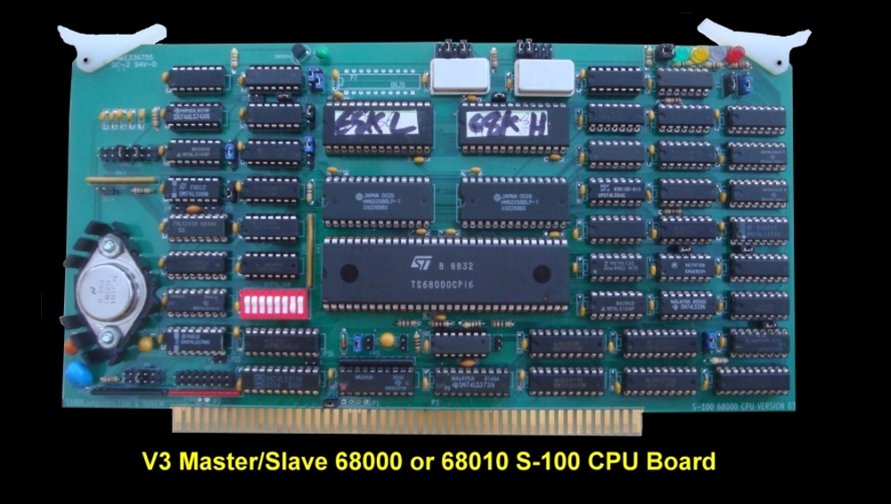
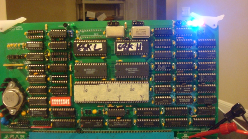
Now the one truly remarkable feature the 68K CPU S-100 board has going for it is the fact that back in 1987 a guy named Alan Wilcox wrote a whole book describing a complete S-100 based 68K CPU board.   The book is the only one of its kind -- describing the construction of an S-100 CPU board, and goes into considerable detail chapter by chapter building up a completely functional board.  The book is an absolute "must read" for anybody building a  68K system.  The title is "68000 Microcomputer Systems Designing & Troubleshooting" by Alan D. Wilcox. Prentice-Hall Inc. Publishers, 1987.  Copies can be obtained from time to time on eBay and Amazon.
On the basis of this Andrew Lynch, Pontus Oldberg, Neil Breeden and Mike Sharkey and I decided to have a go at building a new S-100 68K board.  The first version of this board is essentially a copy of the circuit described in the Wilcox book.  There are a few minor changes but all in all it's the same circuit.  Such a 68K CPU board can only act as a Bus master.  If you had a slave Z80/8086 board it could perhaps co-exist with those CPU's. But the Wilcox board essentially assumes it is the only CPU in the bus.  This is in fact perfectly fine if you only need a 68K based system. 
  
Here is a picture of my build of our first prototype 68K board.

68K CPU Board V1

You will notice the board contains its own onboard ROM's and a little RAM.  It contains a single step circuit to allow you to step through any code the 68K is executing.  What is really nice about this board is that with the addition of a single I/O port on another board for Console I/O you have a completely fictional system with this one board.  In fact by just connecting a power to the S-100 pins you can make the board flash the LED in software out of the bus.  A huge debugging advantage.  The schematic for this board can be seen here.  There are some minor differences from the Wilcox circuit but they are minor.
 
One really neat feature of the 68000 CPU and this board is you can have a basic "freerun" CPU flashing the red LED (address line A20) with a bare board and just a few chips on the board. This is described in detail by Wilcox but essentially with no RAM or ROM on the board and the data lines tied to ground  the CPU sees only 0's on its data in lines.  This is the 68K opcode for:-
   
 
ORI.B   #0,D0

This means move a 0 value byte to data register D0.  With the complete address space filled with 0's that's all the CPU will ever do. It will just increment to program counter and do the same thing again. All the way from its reset address of 0H up to 00FFFFFFH. It will then repeat the process. The red LED is attached to address line A20.  As the CPU cycles through its address space this line will cause the LED to flash on and off.

Here is a picture of the board in this mode along with the schematic from the Alan Wilcox book:-
  
  
FreeRun Board
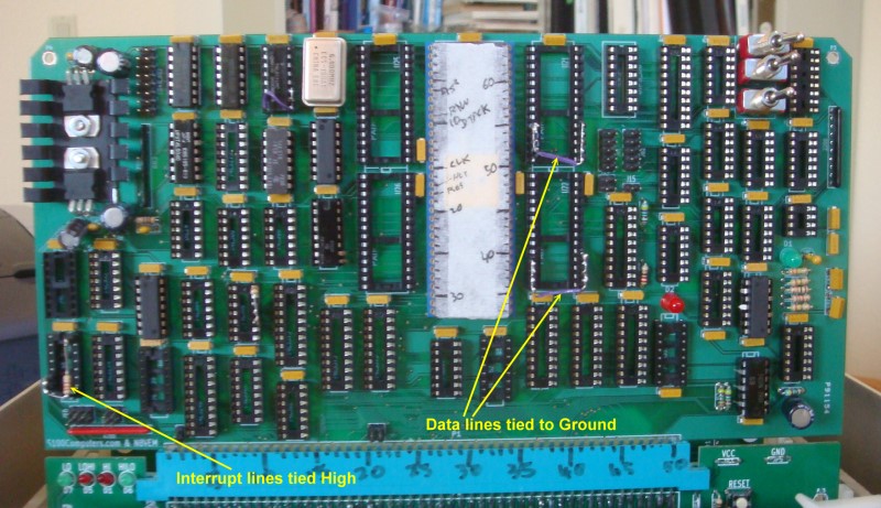
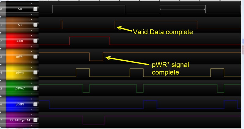
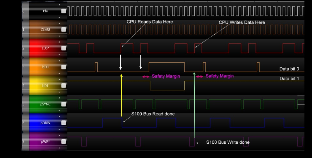
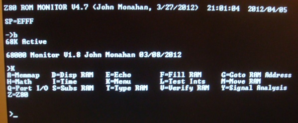
   68000 CPU board in "Freerun" test mode 
Freerun Circuit
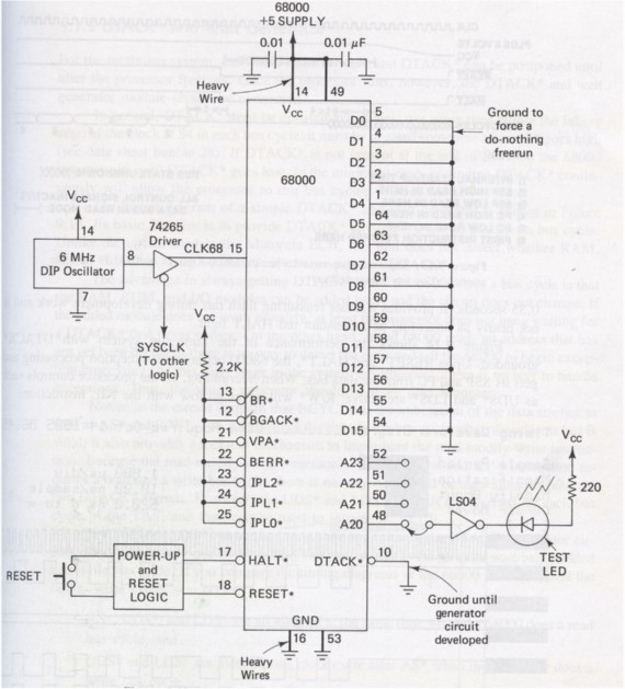
     Freerun test circuit 
  
This is a very simple but useful test for this board. It gives you some assurance your CPU is OK, the reset circuit is working OK and your boards clock generator is working fine.  However you have to be careful to temporally tie high a number of the CPU's input lines as shown above.   The easiest way I found to ground the CPU data lines was to insert a set of jumper pins in the appropriate RAM data pins and tie these to ground.   I checked all the pins in the 68K socket for the correct voltages before adding the CPU chip itself.  You don't want to have the CPU trying to pull a grounded line high.

Next I added the ROM's and support circuit to the board.   I started with two 27128 UV erasable EPROMS. In the past I have found these a bit more forgiving than EEPROMS timing wise -- though (see below), I later quickly changed to 28C256 EEPROMS. UV erasing an EPROM quickly becomes tiresome!

What to code our PROM with.  To answer this you must appreciate that unlike the Intel family of CPU's the 68K starts up at 0H in RAM  -- every time, no exceptions.  In the first four bytes of RAM it expects to find the location for its stack pointer (register A7).   It will always put what is there in A7. In the next four bytes of RAM it expects to find the RAM location for its program counter. With that value it will then jump to any location in its 16M address space.  These locations are hard wired into the chip. So any boot ROM must contain them in its first 8 bytes.  After that you can do what you like, but remember the CPU must start at 0H in RAM.  This is in marked contrast to the Intel CPU line which start at FFFF0H or FFFFF0H.

Our first test code will be real simple, a loop to continuously output to a port a byte value.   We will locate the ROM at 0H in the CPU's address space.  Here is the code we use:-
   
  IO test Code
      
The above code illustrates one major difference between the Intel and Motorola family of chips. On the 68K there are no special control/status signals for the control of I/O ports. As far as the 68K is concerned an I/O port is just another memory location. In order to emulate the S-100 bus port I/O status signals we set aside a block of the 68K's RAM address space for port I/O. The easiest block to use in hardware is the 64K space from FF0000 to FFFFFF.  Clearly way overkill, but with 16 MB of RAM we can afford to be sloppy.  So if the address lines A17-A23 are all high, pin 8 of U10 (a 74LS30, see here) goes low activating the S-100 bus port I/O signals (SOUT or sINP).  Port 01 is my Propeller driven Console I/O board data input port.  An output of 33H to port 01H should place an ASCII "3" character on the screen.
 
Here is a picture of the board with the necessary chips to achieve this test.  You can see the console is continuously receiving the byte value 33H. 
   
  IO Test on Board
   
  68K Debug Output
      
This is a critical test for the circuitry of the board because it is the first time the CPU is talking to the outside world and utilizing the S-100 bus.  It is also very informative at this point to review these signals using a logic analyzer.  Here is a snapshot of one set I took.
    
  Logic Probe Analysis
   
You will note that the S-100 sOUT signal and data lines (A0 & A1) remain valid even AFTER the pWR signal returns high.  This is very important to have reliable data transfers.

Having completed this test I next wanted to install and utilize the boards onboard RAM. The static RAM chips I used were Hitachi HH62256-70ns, (8KX32) chips. Initially the boards RAM was located at 8000H. I wrote a little program to copy the ROM contents (at 0H in RAM) up to that location.  I than wrote a little program to display the contents of that RAM on the CRT.  This is a bit of "ugly" code because I did not want to assume the stack could use valid RAM. The code is therefore inline with no subroutine calls.  The code can be seen here.

Assembling 68K Programs.
There are many good assemblers for the 68000 family of CPU's.  I have been using a fantastic package written some time ago by Tim Larson, Paul McKee and Chuck Kelly called "Easy68K".  It can be downloaded from here.  It runs as its own self contained IDE in windows. Not only does it have a complete assembler but it has a self contained Run and Debug interface.   The only catch is that all console IO goes through the 68k software interrupt Trap #15.  Using this debugger you can quickly write and test code before programming an EEPROM.  The only change being you replace Trap #15 with an output to your Console I/O port.  In all my code examples then you will see some sections commented out to prevent interrupt Trap#15 at runtime.

By comparing the code in RAM with the code in the Easy68K RAM.L68  file you can confirm that the onboard 68K CPU copied the ROM correctly.  Again this is a very important board test,  because from now on we can use a stack pointer and write callable 68K routines.  The EEPROM code for this test can be seen here.

Next we need to get the Boot ROM at 0H in RAM up out of the way to high RAM.  We will use the location 00FD000H-00FD7FFFH.  We will also place the onboard RAM at 00FD8000H to 00FDFFFFH.  This is easily done by carefully configuring the SW2 switch.

The is only one catch, remember the 68K always boots from 0H in RAM.  This is where Alan Wilcox did a neat trick. He realized that the first 3 AS* strobe pulses for data reads by the CPU would always be in low RAM, so he added a 754LS164 counter that forces the onboard EEPROM to address 0 just for that time.  On the fourth AS* pulse the CPU has set stack and PC values, and then unknown to it, jumps back up to 00FD0xxxH (the xxx's were determined by the value loaded into the PC).

I tested this by installing jumper J15 on the board and setting switch SW2 to FDH.   The above code has to be changed. Now the initial PC address long word has to be changed to 00FD0xxxH.  The program will display a memory map of the CPU's address space. The program can be seen here.

With this working correctly I inserted one of our 4M Static RAM boards in the bus.  The RAM showed up correctly in the display.

The next step was to write a simple 68000 specific ROM monitor.  My goal is to model it after the 8086 monitor I wrote.  I wanted to use all the same menu options -- to keep life simple. I should point out that there are a number of excellent well tested 68K monitor programs. The Motorola Educational Computer "Tutor" perhaps being the best known.

As a total beginner I have found understanding this program a little tricky.  If needed it can be seen here. I have opted to write my own. First to learn 68K assembly programming but perhaps more important it will allow me to more easily later splice in code (as I have in the 8086 monitor) to run diagnostic tests on our IDE and ZFDC controller boards.  This should help a lot getting CPM-68K up and running.

The 68000 monitor program is "a work in progress".  The Windows emulator Easy68K has been very useful in laying its groundwork and initial debugging.  The most up to date versions can be obtained at the bottom of this page.  Here is an example of it displaying a memory map and showing the monitors (current) menu options.
   
  Memory map
   
As I said above the Wilcox board functions as a S-100 Bus master.  I decided to do a second board that has circuitry (similar to the 8086 board) that will allow the 68000 CPU board to run as a slave board.  This has turned out to be more difficult than you might expect because there is little spare room on the board. 


A FINAL PROTOTYPE 68000 CPU BOARD
Much was learned from the above board.  It worked very reliably at 6MHz but was unreliable above that.  It was also restricted to being a Bus Master board. In other words it could be the only controlling CPU board in the S-100 Bus.  Utilizing much of what we had learned with the Master/Slave 8086 CPU board a second prototype board was constructed that allowed the 68K CPU board to be configured as a Bus Master or a Bus Slave. In the latter configuration for example the system could be booted up with a Z80 and when required, control switched over to the 68K CPU board. Control can later, if required, be switched back to the original Z80 CPU which will pick up where it left off. You can write code to switch back and forth between the two CPU's continuously.
 
Here is a picture of this prototype board:-
 V2 68K Board
  
As you can see some further changes were required to the board. These will be corrected in the final production board.
The schematic of the final board can be see here.  Amongst the changes were:-

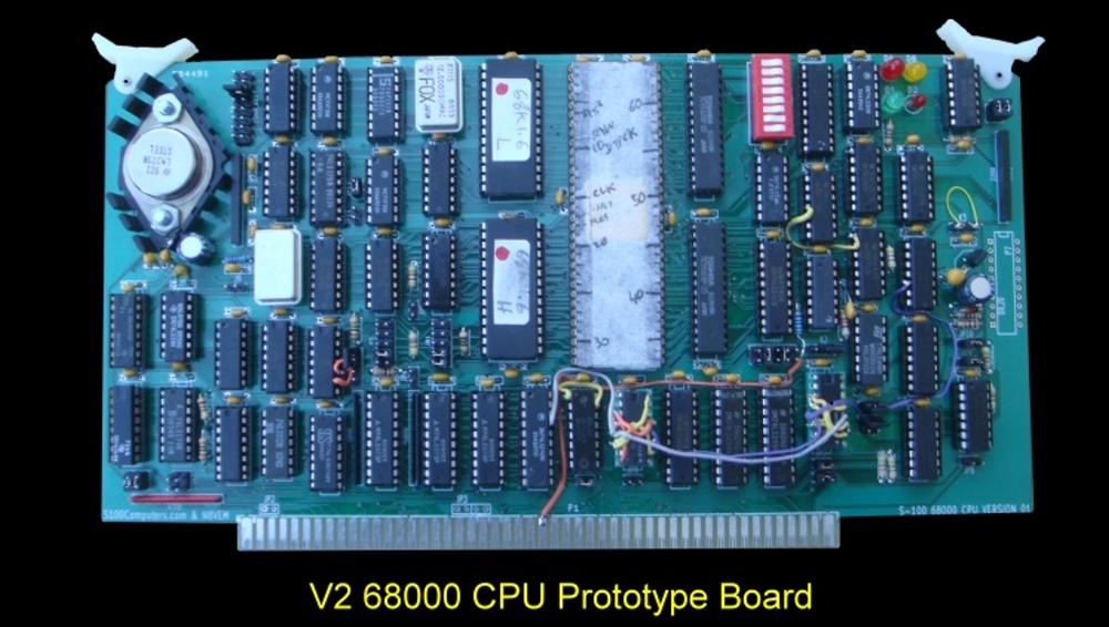
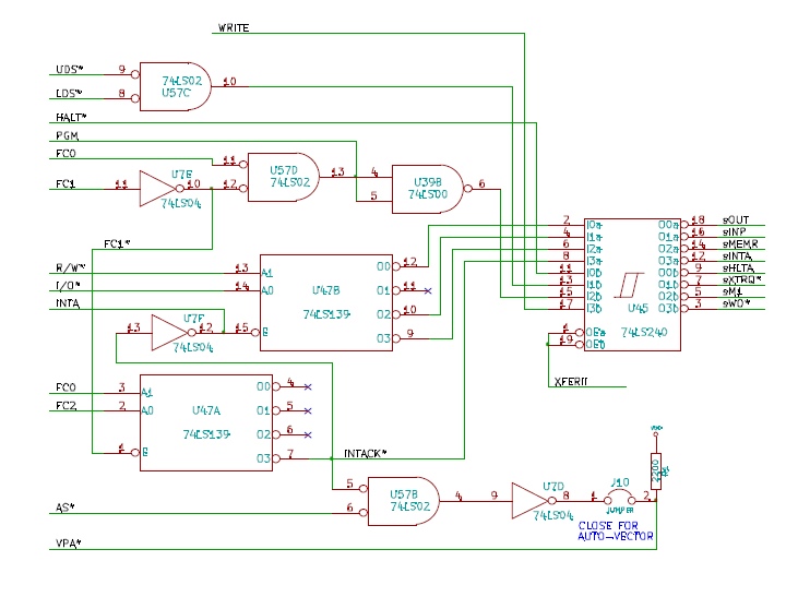
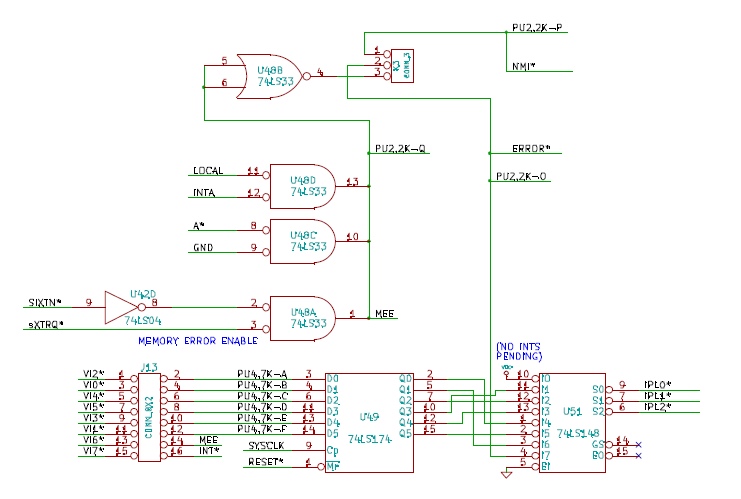
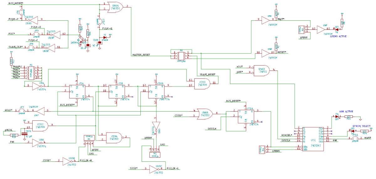
  Added switching/handshake circuit to allow S-100 bus Master - Slave bus switching
  Removed hardware switches and single step circuit. Stepping can be done with the SMB
  Selected use of 74Fxx chips for up to 7MHz S-100 Bus clock speeds
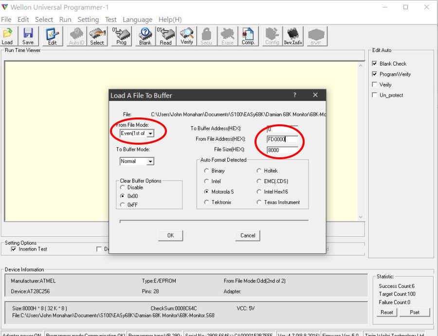
  The board can now utilize 28C256 (32KX8) EEPROMS
  More LED's to show what is going on. Board active, EPROM active, Supervise Mode

The board in my hands will work (at 7MHz - see below) with any of the S100Computers boards  we made over the years. At high speeds however, I find that unlike our Z80 and 8086 boards, it really works best (less wait states required), with our 4Mg Static RAM board immediately beside it in the bus. I recommend this configuration if possible. Also at high speeds it does not run reliably in an extender board.  There are a lot of traces on this board. These observations may disappear in the final optimized board.

For the board to run at 7MHz it has to be jumpered for  two wait states for I/O in order to utilize I/O ports on other S-100 boards and 3 wait states for the onboard EEPROM.  Also for reliability a number of the 74LSxx chips need to be changed to the faster 74Fxx types.  In particular chips related to the wait state/DTACK* (see below)  circuitry.  Change U36, U31, U41, U33, U34, U46, U35, U36, U37, U38. Also if possible (they are not that common), U14 & U55.  Also U30, U31, U7, U39 and U35.  Use 74Fxx or 74Sxx chips.

About the Circuit
Alan Wilcox has done an excellent job in explaining the core circuitry of this board. If you can obtain a copy of this book do so.   The 68000 CPU interfaces to the bus in either 8 or 16 bit modes.  To understand how the S-100 bus data lines are handled in 8 and 16 bit modes please see here.  While the 68K can read or write to odd and even addresses in 8 bit mode, in 16 bit mode it will always read on an even address boundary. A 16 bit odd address read or write in not possible with the 69K CPU.   This simplifies the bus access considerably.   The CPU supplies two pins (UDS* and LDS*)  to flag if an odd, even or both 8 bit data bytes are required.
  
  RW Circuit

As explained above the 68K initializes from a reset state at 0H in memory.   To avoid placing a ROM in low memory the circuit counts the initial first 4 address  line strobes (AS*)  and then jumps to high RAM (in my case 00FD0000H, set with SW2) where 32KX2 or ROM is located. At 00FD8000H 32KX2 of fast static RAM is also located.  The onboard ROM/RAM will lower the LOCAL* line.  This line is used to switch off the S-100 bus data drivers within these ranges.    Any 68K address line equal to or greater than 00FF0000H will be configured on the S100 bus as an I/O port.  IC U10, a 74LS30, handles this function.
 
  ROM_RAM Select Circuit
   
As mentioned above it is very important to appreciate that unlike the Intel/Zilog family of CPU's, the 68K CPU (and family), always wait for a memory or I/O device signal to acknowledge its presence before the CPU sends the actual R/W strobe signals.   If the CPU accesses a device for example and it does not receive a returned DTACK* signal (on its pin 10) the CPU will hang indefinitely.   By delaying the length of time DTACK* is returned to the CPU we can add wait states for slow RAM or I/O devices. Up to 8 wait states can be added for any I/O cycle, an M1 S-100 bus cycle, or an on-board ROM/RAM access cycle on this board.  The circuit to implement this can be seen here:-  
  
  Wait Circuit
  
There is an exception to the above process however, if the hardware pulls the VPA* line (pin 21) low the 68K assumes the hardware is immediately ready.   This signal in fact is uses a lot by Motorola I/O chips such as UARTS etc.

In order that the CPU does not hang, a simple "watchdog" timer circuit is included on the board. If the CPU times out, the S-100 bus ERROR" line is activated with the following circuit. This circuit is normally never activated.
  
  Watchdog Circuit
 
The generation of the critical S-100 bus status and control signals are generated by looking at the 68K CPU FC0, FC1, FC2, UDS*, LDS*, and the R/W signals.  The circuitry here is unfortunately a bit complex.  Here is the circuit for the S-100 status lines:-
 
  Statu Lines
 
The way the 68K handles interrupts in my opinion is far more logical and easier to work with in hardware that for the Intel CPU's. You don't need a separate 8259A like interrupt controller.  Instead you feed the interrupts into the CPU directly (in a 1 of 8 combination) to its three dedicated interrupt lines (IPL0, IPL1, and IPL2).  Programming is easy as well.  The default interrupt vectors are at eight 32 bit addresses starting at 64H in RAM up to 7CH in RAM.  In the simple 68K monitor described below, if you hit the "L" the screen the program will display which of the S-100 Bus interrupt lines are triggered.

Interrupts can be handled in two ways.   In the simplest format,  one or more or the IPL0-IPL2 lines force the CPU to the above low RAM interrupt vector locations. 

There is a second hardware option where the hardware can place its own vector number on the data bus (like an 8059A).   The 68K CPU generates the Intel equivalent of an Interrupt Acknowledge signal by holding FC0, FC1, & FC2 high.  This is the only time these three lines are high.   That is the signal for external hardware to put a vector on the bus. When ready, then hardware must pull VPA* low for the CPU to read the data lines (all 16 if required).   While not commonly used, this provides an extremely powerful and fast interrupt structure.

For our needs we will utilize the simple interrupt vector lines the S-100 bus provides.  The circuit is shown here.
  
  Interrupts Circuit

The highest priority interrupt, NMI*, pulls IPL0, IPL1 7 IPL2 all high going to pin 4 of U51. This line can also be used for the bus ERROR signal.  The most common use of this interrupt would be if a 16 bit access to an 8 bit board did not return the SIXTN* acknowledge signal.

Finally there is the master/slave bus switch-over circuit.  I borrowed the tried and true reliable circuit we have on our 8086 board.
This board upon power on or reset will normally exist on the S-100 bus as a slave CPU board. That is it will be inactive while the Master CPU (usually a Z80) board is active. (It can be configured as a Bus Master itself, but lets pass on this for now).   Please look at this diagram:-
   
  Switch Circuit
 
As setup the 68K CPU is held in a "HALT" state (pin 17 is low) on power up.  The S-100 bus allows for up to 16 slaves (CPU/DMA) boards. They are selected by the four S-100 lines TMA0-3 (pins 55-57 & 14).  I will use the TMS0 line here.  To activate the board we lower TMA0 (typically by outputting a bit from a port elsewhere on the bus, e.g. the SMB, but this could even be a bounce less switch).  This lowered signal is passed along step by step the three 74LS74 flip flops U2A, U2B, U30B & U71A are clocked by the S-100 bus master clock Phi.  The output from flip flop U2A is sent back to the bus as a low on the S-100 line HOLD* (pin 74). This tells the Z80 another board wants the bus. When it is ready, it raises the S-100 hold line pHLDA which clocks the flip flop U2B. This is then clocked (by Phi) through flip flop U30B and eventually raises the HALT* pin 17 on the 68K. This releases the 68K from its halt state. The output of flip flop U30B also puts out the important signal XFERII which amongst other things allows the "new" Phi clock signal for the 8086 to appear on the bus.  Meanwhile at this time all the Z80 status, data, address and control lines are tri-stated.  It's as if the Z80 no longer exists on the bus.

Now it should be pointed out that the original IEEE-696 specs allow for only 1 master clock on the bus. In real world practical systems this usually meant the Z80 clock.  It was not long however until almost every S-100 board manufacture  adapted a modification (like that above) that allowed the slave CPU to supply its own (faster) clock.  This is what I will use in all our Slave S-100 boards.  It is important also to remember that this board cannot itself transfer control to another slave board (for example a DMA controller) the board/software must refer back to the true S-100 bus master.  This is how the IEEE-696 protocol was setup.  

However because both the Z80 and 68K CPU are held in halted states one has complete flexibility going back and forth between the two CPUs (or a third DMA controller board! -- a future project).    The board has a number of jumpers to allow it to be configured as a bus master as well. It could for example control an external DMA controller with suitable handshake circuitry.

Unlike our 8086 board there was not enough room on this board to include an I/O port to switch one of the S-100 bus TMA lines.  If you have our SMB board there is a port directly hooked up to the S-100 bus TMA0 and TMA1 lines.  However one bit on any S-100 I/O port on any port can be used.  Remember TMA lines 0,1,2 & 3 are open collector lines, so one totem pole 74LSxx gate only please, or use an open collector gate.   Alternatively just hook a bounce less switch to one of the boards P5 jumper pins.

Analysis of S100 Bus Signals
To have a stable system at these speeds it is very important that the key S100 bus signals are within specs for the 68K CPU.  The critical signals are the read and write signals when the CPU is getting or putting data on to the bus.  It is absolutely essential that the read and write strobes are well within the window in which the data is stable on the bus.   For the 68K the rise of the UDS* and LDS* signals (pins 7 & 8) is the exact time the CPU reads data from its data pins, or the longest time data is stable when writing data.  An analysis of the signals on this board shows that the data windows are well within the required range.   Likewise the S-100 signals pDBIN and pWR* have a good safety margin. Please see the signal analysis below.

pDBIN & pWR*


Step By Step Build Instructions of the V3 68K CPU Master/Slave
S-100 Board.
Here is a picture of the final V3 68K Board.
 
  Final V3 68K Board
      
T
he first step is to examine the bare board carefully for scratches or damaged traces. Use a magnifying glass if need be. The quality of the boards we get is excellent. I must have done about 30 by now and never had a problem, but there is always a first time. A broken trace is almost impossible to detect by eye on a completed board.  This 68K board is one of the densest board we have done. The traces are often close and fine. Be careful not to scratch the board.  One or two of the traces run down between the S-100 bus gold pins. Check they do not make contact with the bus pins in your system.  The should not.

Next solder in all the required IC sockets, resistors, resistor arrays, capacitors and jumpers.  Let's start with an 8 MHz Oscillator (and the 2MH clock Oscillator). Add SW2 and the voltage regulator.  Note there are several traces under the position of the 5V TO-2 voltage regulator.  It's important to have a mica washer between the board and the bottom of the heat sink to prevent ground shorts. 

Be sure you put the resistor arrays in with the correct orientation of pin 1. Check their values before  soldering (they are difficult to remove). 

For prototype boards I generally use "double swipe" IC sockets. For a final board like this I prefer to use "Machine Tooled" IC sockets.  However they are more expensive and you have to be particularly careful not to bend the IC pins.  If you think you will be doing a lot of EEPROM burning you should use the Low Profile ZIF sockets (e.g. Jameco #102745) for the EEPROM socket.  The two clock oscillators should have their own special sockets (e.g. Jameco #133006).  I like to add a smear of solder to the oscillator pins to ensure a tight connection. It's also fine to solder the 2MH oscillator directly to the board since it never will change.

Check the voltage to sockets on the board is above 5V by placing the board in your S-100 system using an extender board. With no load you will typically get 5.00V  (+/- 0.25V).  BTW, your system should boot and run correctly with its Z80 CPU. If not, you have a serious solder bridge somewhere on the board.  Before you do anything else with a magnifying glass go over every socket on the board and examine for proper solder joints. I like to "reheat" each joint just to be on the safe side. The silk screen/varnish on these boards is quite thick. It's easy not to have a good solder joint for the ground pins.  Double check.   Extra time here will save you hours later! 

Next add the four LEDs. Before you solder in each LED check it lights up by grounding the appropriate pins on the socket of U72, U9 or U8.  Here is a picture of the board at this stage.
  
  Initial Setup V3
   
 
We will now build the board up in functional steps. Avoid the temptation of adding everything at once and popping it into your S-100 box.
Step by step is faster in the end -- trust me.

We will first setup the board as a bus master first. Once this is working we will reconfigure it as a S-100 bus slave.  As a master you need to remove any other CPU's in your system. In fact its best to start with a system consisting of only a video and/or console I/O board. I use the Propeller drive Console IO board. It's also convenient to have a front panel. I use our SMB.  In any event you need to determine if your S-100 system generates the reset, POC and Slave Clear signals or if you need them generated on this board.  If so, you will need to add the jumpers JP6, JP9, JP8 and JP10 and U69.   If these signals are generated elsewhere, its important these jumpers are not used.

Start by adding U30, For IC socket U51 add another blank socket  with pins 6,7 and 9  tied high via a 1K resistor to pin 16.   This insures the CPU will receive no interrupts.

Add U66 and U9.  Jumper P6 5-6 and 1-3. Jumper K6 2-3.  Add U8, jumper K7 2-3 and K6 2-3.  For IC socket U34 add another blank socket  with pin 6 tied to ground (pin 7).

Next carefully construct two 28 pin blank sockets with their pins 11, 12, 13, 15-19 tied to ground. Carefully insert these sockets in sockets U25 & U26 on the board. This will ensure the data lines going into the CPU will be zero on all data lines.

Insert the board into the S-100 bus. Check the pins on U24 are consistent with the CPU running in "freerun" mode as described above.
    
  Freerun Mode
 
There should be a continuous pulse on pin 15. Pins 17 & 18 should pulse low on reset but then return and stay high.
Next carefully add the CPU itself and power up the system.  LED D2 (mode) should flash on/off about once a second continuously.  It is critical you get this to happen before going any further.  Here is a picture of the board at this stage.
  
  V3 Freerun
    
Next we will stepwise add the various CPU support circuits.  We will all the time feed the CPU 0's on its data lines to keep it in "freerun mode".

First we will add the DTACK* and Wait state circuitry.
Add U36, U34, and U31. Temporally bend out pin 9 of U31. Add U33, U41, U46, and jumper JP13.
Temporally jumper together 11 & 12 of U46 and ground pin 10 of U33.
Add jumpers on P2 for 11-12 and 8-7. Add U10.  

Insert the card into the S-100 box.  The 1 second flashes of D2 should continue. Remove the U46 and U33 jumpers.
The flashes should continue but be a little faster.
If you have a SMB pressing the stop button will stop the flashing, release and the flashing should continue.

Add U35 and U37. Check again for freerun so LED D2 flashes.
Next add U38, U42, U40 (use a 74367 rather than a 74LS367). Add jumpers JP12 and  K1 2-3.  Check for LED D2 flashing.
Check U40 pin 7 is high and 7, 9, 11 and 13 all pulse low continuously.

Next add U57, U7,U47, U45 and U72.
Jumper K1 2-3, K2 1-3 (with wirewrapp) and  K4 2-3,
Add JP10 and JP11.
Next add U27, U28 and U32.
Place the card in the bus and power-up. Now not only will LED D2 flash but the address line HEX display on the SMB will cycle from 0 to FFFFFFH.
Here is a video of the board at this stage:-


Next we will add the Watchdog timer and Interrupt circuit.
Insert U50 and J9. Insert U48, U49 and U51.  Jumper K3 2-3.  
Check the board again for LED flashing.  There should be no pulses on U51 pins 6,7 and 9.

Next we will add the EPROM/RAM board circuitry.
Add U15 and switch SW2.   The default position  for SW2 is all switches open except position 7. This gives a EPROM address of
11111101 or FD0000H.  Add U12, U11, U16 and U17.
Jumper J14 1-3 and 2-3 (both jumpers are vertical).  Check for the usual LED flashing. Pin 19 of U15 should pulse about every 8 seconds.  Next add J15.
Next add U13.  In the LED flashing test  pins 3 and 6 of U13 should pulse low while pins 8 and 11 remain high.

Remember the default 68K monitor configuration (see below) has the monitor residing at FD0000H, the onboard RAM at FD8000H and the S-100 Ports at FF0000 to FFFFFFH.

Now remove the grounding sockets in U25 and U26.
Add U39, U14 and U55.  Bend back pin 9 of U31 that we did way back at the start of this build.
Jumper JB1 1-2 and 3-4.  Jumper JB2 3-4 and 7-8. Add the two static RAM chips U21 and U22. (HM62256's, Jameco #42876)
and EEPROMS U25 and U26 (28C256's, Jameco #74843)
Add U18, U19, U20 and U23. 
Make sure the Even Byte EEPROM is in U25 and Odd byte prom is in U26.  (I'm assuming everybody knows what this means. If not, carefully consult your PROM programmer manual or ask around).

If you have the 68K monitor programmed into the 28C256 EEPROMS,  the monitor should signon at this stage.
 
  68K menu
  
 
Here is a picture of the board at this stage.
    
Monitor test
  
If you have a Wellon EEPROM programmer here is a picture of the burn menu.
    
  68K ROM Burn
 
Remember Motorola files are not .HEX files they are .S68 files. Alsoyou must burm the High and Low ROMs seperatly to reside at FD0000H.


A 68K Monitor
The 68K monitor for this board can be  see here     It is modeled after the 8086 monitor.  The same command structure is used.  
In July 2020 the boards  68K monitor was updated by Damian Wildie to run a diagnostic menu  for our  IDE./CF card  board. This should facilitate bringing CPM68K with the board.  Some volunteers would be great to help in this process.


Configuring the V3 68K board as a S-100 bus slave.

Configuring the board as a bus slave is the most often used configuration of this board. This allows you to bring up your system, for example with CPM and a Z80 and later switch control over to this 68K board.

To reconfigure the board as a bus slave continue where we left off above.

Add U2, U70, U71 and U69. The board should now have all sockets full.
Set the jumpers as follows.
P5 5-6, P6 1-3 and 4-6,  K4 1-2 and K5 1-2. Add jumper K5 1-2.
For a slave configuration  K1 3-4 , K2 2-3.  

With P5 set 5-6 this board will take command of the S-100 bus when the TMA1* line (S-100 pin 56) goes low.  If you have our SMB, inputting from port EC will do this (using my Z80 monitor "B" command) and the appropriate SMB jumper.  If you do not have this arrangement, use some port that will lower one of the input line on P5. A crude way is just to manually ground a pin (a bounce less switch being preferable).

In any event with pin 1 of U8 low the cascade of handshaking events will take place switching control from (typically) the Z80 to this board.
This switching cascade has by now been well tried out in everything from a 6502, 8088, 8086, 80286 and 80386. There should not be a problem here.  It is described in a little more detail for the 8086 CPU board.

Note with our SMB, inputting again from port EC will return control back to the Z80.  Software can be used to go back and forth between both boards.

One other point.  If you intend to have multiple CPU's in your S-100 bus you have to be careful not to load down the open collector lines (in this case those to RR4 & RR5) with low resistor values such that on multiple boards the pull-up value could be reduced to ~100 ohms.  This will tax the drivers and slew their output.   In situations like this I usually add a single line socket (0.1" centers, Jameco #104054, cut to size), and either do not insert a resistor pack or use one with a high value like 4.7K.

For a single master board setup of course use 1K pull-ups.

The board is currently running in a 21 slot S-100 bus system with a 12MHz Oscillator.  No wait states are required for our 2MG static RAM board and two wait states for all S-100 Bus I/O.  So jumper P2, 3-4.  If you have other S-100 IEEE-696 RAM boards your setting may be different.

Test RAM Read/Writes with the two 68K Monitor commands
M0,FFFF, 12345
V0,FFFF,12345

There should be no errors what so ever.


A Production Board
Realizing that a number of people might want to utilize a board like this together with a group of people on the  Google Groups S100Computers Forum, "group purchases" are made from time to time.  Please see here for more information.

A third production run of this board was done on (1/18/2016) call 68K-V3A.  This board is essentially the same as the above board except the Silkscreen has more information and two jumpers (K8 & K9) were added to accommodate the special situation where this CPU board would act as a slave of a slave in the S100 bus. See here. The normal configuration of these jumpers is K8 1-2,  K9 2-3.  Please note the Silkscreen label on this board reads:- "S-100 68000 CPU VERSION 1.03B"

Please note there the file names for this board are labeled V1 but the actual board is named V3.  All the files below are for the final V3 Board.

The links below will contain the most recent schematic of this board.
Note, it may change over time and some IC part or pin numbers may not correlate exactly with the text in the article above.


EASY68K SOFTWARE (11/14/2011)
MOST CURRENT 68000 CPU BOARD ROM MONITOR SOURCE CODE.ZIP File
   (V3.0  2/6/2024)

MOST CURRENT 68000 CPU BOARD SCHEMATIC  (V3,1 FINAL PRODUCTION RUN, 3/16/2013)

MOST CURRENT 68000 CPU BOARD LAYOUT       
(V3,1 FINAL PRODUCTION RUN, 4/7/2024)

LIST OF BOARD ITEMS  (V3.1 FINAL PRODUCTION RUN, 11/19/2013)

Most current KiCAD files for V3B  board   
 (68K V3A.zip  (V1.03B) 4/7/2024) 


Other pages describing my S-100 hardware and software.
Please click here to continue...


This page was last modified on 02/07/2024